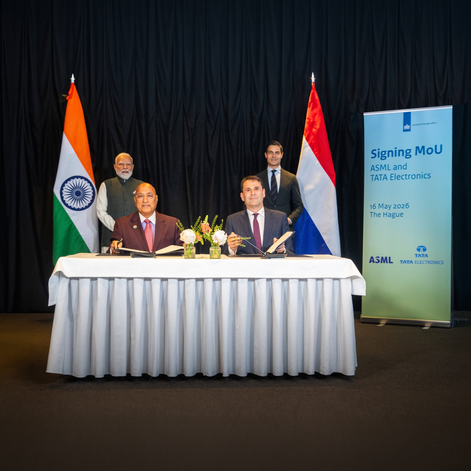

Tata Electronics is expanding its global technology partnerships for an $11 billion semiconductor fabrication plant in Dholera, Gujarat, bringing Dutch chip-equipment giant ASML alongside Taiwan’s Powerchip Semiconductor Manufacturing Corp. as India pushes to establish its first commercial 300 mm semiconductor fab.
The Dholera facility is being developed by Tata Electronics in partnership with Taiwan-based Powerchip Semiconductor Manufacturing Corp. (PSMC), which is providing technology and execution support. The plant is designed for capacity of up to 50,000 wafers per month and will manufacture chips for automotive, computing, communications, data storage and artificial-intelligence applications.
Tata’s partnership with ASML adds one of the semiconductor industry’s most important equipment suppliers to the project. Under a memorandum of understanding announced in May, ASML will provide its lithography tools and related solutions to support the establishment and ramp-up of the Dholera fab.
ASML to Support Lithography and Production Ramp-Up
Lithography is a critical stage of semiconductor manufacturing in which circuit patterns are transferred onto wafers during chip production.
ASML and Tata Electronics said their collaboration will extend beyond equipment. The companies plan to work on local workforce training, lithography-intensive skills, supply-chain resilience and research infrastructure intended to support the fab over the longer term.
The agreement also reflects growing semiconductor cooperation between India and the Netherlands. ASML is headquartered in the Netherlands and is one of the world’s leading suppliers of lithography systems used by semiconductor manufacturers.
Powerchip Provides Manufacturing Technology
PSMC plays a separate and fundamental role in the Dholera project.
Under its agreement with Tata Electronics, the Taiwanese chipmaker is providing design and construction support, licensing semiconductor manufacturing technologies, assisting with engineering and technology transfer, and helping train Tata engineers at its facilities in Taiwan.
The partnership gives the Dholera fab access to a technology portfolio covering 28nm, 40nm, 55nm, 90nm and 110nm process nodes, according to Tata Electronics.
These technologies can support chips used in applications ranging from power-management integrated circuits and microcontrollers to display drivers and high-performance computing logic.
$11 Billion Investment in India’s Semiconductor Industry
Tata Electronics plans to invest approximately $11 billion (₹910 billion) in the Dholera facility, which the Indian government has designated as the country’s first commercial semiconductor fabrication plant.
The project is part of a broader effort to establish a domestic semiconductor manufacturing ecosystem in a market that has historically depended heavily on imported chips.
Tata is building partnerships across equipment, process technology, design, materials and workforce development as it prepares the facility for production. Its semiconductor network includes PSMC and ASML as well as collaborations with other international technology companies and research institutions.
First Chip Targeted for Late 2026
The first chips from Dholera have previously been targeted for December 2026. India’s electronics and IT minister said when the project was launched in 2024 that the first semiconductor output from the facility was expected by that date.
However, Tata Electronics and ASML’s May 2026 announcement described construction as progressing and focused on establishing and ramping the fab without confirming December as the start of commercial-scale production. The December date should therefore be viewed as a production target rather than confirmation that commercial operations will begin that month.
Once operational, the Dholera fab would give India domestic front-end semiconductor manufacturing capacity while linking Tata Electronics with major suppliers of manufacturing technology and equipment from Taiwan and Europe.